Openair-Plasma® in Semiconductor Packaging
Openair-Plasma® in Semiconductor PackagingPlasma cleans and activates surfaces inline, quickly and in a controlled manner. In the semiconductor industry in particular, this enables highly particle-free process control, which reduces waste and increases quality. In addition to perfect adhesion and optimal wettability, service life and product stability also benefit: interface failures such as delamination (IDM) or internal cracking (CCM) can be significantly minimized through targeted plasma pretreatment.
Interface quality is crucial
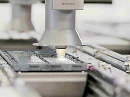
Plasma cleans and activates surfaces inline, quickly and in a controlled manner. In the semiconductor industry in particular, this enables highly particle-free process control, which reduces waste and increases quality. In addition to perfect adhesion and optimal wettability, service life and product stability also benefit: interface failures such as Interface Delamination Mode (IDM) or Cohesive Cracking Mode (CCM) can be significantly minimized through targeted plasma pretreatment.
Modern semiconductor products consist of complex multi-material systems—from metal/metal to metal/polymer to various polymer combinations. Their reliability depends crucially on how cleanly and permanently the material interfaces are bonded. Even the smallest defects at these interfaces lead to delamination, cracks, or unexpected failures.
Four main factors can compromise the quality of this critical interface. Oxides that form in undesired areas can hinder proper bonding and electrical contact. Poor surface wettability prevents uniform adhesion and reliable material flow during the joining process. In addition, contamination by particles or residues can create defects that weaken the connection or lead to premature failure. Finally, differences in the coefficients of thermal expansion (CTE mismatch) can cause mechanical stress and microcracks during temperature changes, further reducing the long-term reliability of the interface.
All these challenges can now be effectively addressed with plasma technology—without the use of harmful chemicals, cost-intensive vacuum technology, or expensive specialty gases.
Wafer Cleaning—Atmospheric-pressure Plasma, Maximum Purity
Advanced semiconductor devices start with the purest wafer surfaces, since every process step depends on them. Silicon wafers, chips, and high-performance semiconductors are extremely sensitive— even the smallest contamination can affect performance and yield. Traditionally, wafer cleaning required low-pressure plasma systems in sealed vacuum chambers.
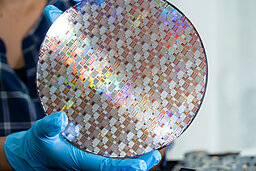
The advent of Openair-Plasma® technology has transformed this: now, atmospheric-pressure plasma achieves nano-level surface cleaning inline—without a vacuum or production delays. By eliminating the vacuum step, Openair-Plasma®simplifies workflows and enhances automation. Wafers can move directly from slicing and polishing into plasma treatment, achieving complete removal of carbohydrates and particles. The result: fewer errors, faster production, and greater process efficiency.
This non-vacuum, inline plasma process ensures maximum surface purity for all semiconductor materials. It provides reliable and repeatable cleaning without the use of chemicals and without production downtime. The technology can be easily integrated into automated manufacturing lines, contributing to lower production costs while simultaneously reducing environmental impact.
Result: Every wafer enters the packaging workflow perfectly prepped—for wire bonding, die attach, or any next step—guaranteeing superior device reliability from the very beginning.
Die Attachment and Interconnection
A perfect connection is at the heart of every modern semiconductor packaging process. Contaminated, poorly prepared surfaces lead to bonding errors, delamination, “non-stick on pad” and premature failures.
In processes such as wire bonding, die bonding (flip chip) and modern adhesive bonding, the quality of the surface determines reliability and performance.Openair-Plasma® cleans and activates all critical surfaces—substrate, bond pads, chip/die. Oxide layers and disruptive residues are removed, and wettability and adhesion are optimally adjusted.
Lead Frame—Oxide Reduction
Oxide layers on metal lead frames can weaken or prevent strong, reliable connections in semiconductor devices. With Openair-Plasma® and the REDOX® tool, these unwanted oxide layers are removed inline, dry, and without vacuum chambers, seamlessly integrated into the production process. The result is improved bond quality—both electrically and mechanically—along with higher production yields, reduced waste, and consistent, repeatable surface conditions for maximum process reliability.
Die Bonding—Why is plasma indispensable before the die attach process?
The quality of the die attach process is crucial for the reliability and performance of every semiconductor device. Uneven bonding, voids, or poorly adhering dies can compromise functionality from the first use to the end of the device’s service life. Openair-Plasma® ensures that every die and substrate starts perfectly: organic residues and oxide layers are fully removed inline, and surfaces are precisely activated—without vacuum or aggressive chemicals. The difference is clear: without plasma treatment, voids, delamination, and adhesion issues occur more often, whereas with plasma, every die is bonded securely, firmly, and cleanly.
The benefits include maximum process reliability and bond quality, clean removal of all contaminants, and improved adhesion for adhesives, epoxy, and solder. Perfect wettability reduces voids and delamination, ensuring reliable device performance even under thermal and mechanical stress. This leads to higher yield, less waste, and consistent product quality.
In short, with Openair-Plasma®, every die attach step becomes a technological masterpiece, delivering semiconductors that perform flawlessly under all conditions.
Wire bonding—Maximum reliability through plasma activation
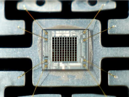
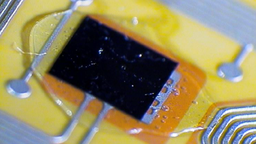
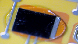
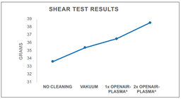
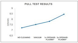
A perfect wire bond connection is the backbone of every modern IC—and it starts with an absolutely clean, activated surface. Even the slightest residues such as oxides or organic contaminants lead to “non-stick on pad,” weak shear strength, or even premature failure.
Only plasma activation creates the necessary conditions: contaminants are completely removed, and the bond pad surface is maximally activated. This not only ensures a stronger wire grip, but also reliable electrical and mechanical stability. Defects such as weak bonds, bond lift, or costly rework are dramatically reduced. The result: higher yield, stable and repeatable results—and a decisive quality advantage in every packaging workflow.
Thermo-Compression Bonding (TCB)—Plasma ensures perfect flux-free connections
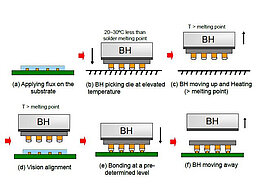
With the Openair-Plasma® and REDOX® processes, you create the ideal conditions for even the most demanding bonding applications—ensuring reliable advanced packaging and high-end performance. These innovative surface treatment technologies enable stable, void-free connections without the need for flux, providing maximum process reliability and repeatability. At the same time, they support environmentally friendly and cost-efficient production, while delivering superior electrical and mechanical reliability for long-term performance and product quality.
Plasma before fluxing
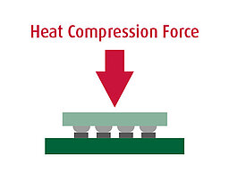
In Thermo-Compression Bonding (TCB), the quality of the surface determines the reliability and performance of the entire connection. Plasma treatment prior to fluxing creates a uniform, high-energy surface and ensures optimal wetting behavior. This significantly reduces the amount of flux required, making bonding more reliable and measurably increasing the reliability of the device.
Fluxless TCB
The removal of metal oxides is particularly important in flux-free TCB processes. Here, Plasmatreat's REDOX® technology offers automated, inline-capable plasma reduction: metal surfaces are completely cleaned and activated during the ongoing production process, and oxide layers are removed—without the use of chemicals or wet processes.
Encapsulation Preparation
Stable, long-term reliable protective encapsulation is the backbone of modern semiconductor components. However, even the best encapsulation material can only achieve its full effect if the surfaces are optimally prepared. Invisible residues, oxides, or poor wettability quickly lead to delamination, air pockets, or defects—thus jeopardizing the electrical performance and long-term stability of the package.
Targeted plasma activation prior to encapsulation creates perfect surface conditions: The encapsulant can be distributed reliably and without bubbles, adheres to all relevant materials, and thus ensures long-lasting and comprehensive protection—even under the most demanding conditions.
Activation Before Underfill
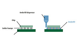
High and uniform surface energy is the key prerequisite for underfill materials to wet reliably and flow seamlessly. With Openair Plasma®, substrate surfaces are activated directly in the inline process, ensuring that the underfill is optimally distributed and adheres reliably. At the same time, even the finest particles and residues from the dicing step are thoroughly removed. The result: perfect fillet formation, significantly fewer air pockets (voids), and encapsulation that provides maximum reliable protection in everyday use and under stress.
Surface Preparation for Molding and Encapsulation
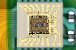
The surface quality of the substrate is critical for reliable molding and protective encapsulation. All materials involved—from lead frames and fine wires to advanced encapsulants—must be thoroughly cleaned, free of oxidation, and highly reactive. Only then can seamless material flow, maximum adhesion, and long-term stability be guaranteed.
Openair-Plasma® offers a range of specialized processes to achieve this. Plasma cleaning removes all organic and inorganic residues that could compromise adhesion or cause delamination. Plasma reduction eliminates even the finest metal oxides, creating highly active surfaces that are chemically bondable. PlasmaPlus® Nano Coating applies a thin, uniform barrier that protects against moisture while enhancing material compatibility.
Together, these processes ensure optimal flow of potting materials, prevent air pockets, and enable full compliance with REACH and MSL1 standards, delivering maximum reliability even under the most demanding production and operating conditions.
Nano coatings for optimum EMC adhesion

For particularly demanding packaging applications, nanoscale plasma coatings ensure optimum bonding between epoxy mold compounds (EMCs) and the prepared substrates or dies. The result: superior adhesion, maximum reliability, and consistent performance—even under the highest thermal and mechanical loads. These nano-coatings create precisely tailored, highly active surfaces that effectively prevent delamination and cracking. This keeps the package stable and durable—from the first functional test to years of field use. Fewer defects, more output—and consistently high quality.
Barrier Coatings—Protection at the atomic level for sensitive ICs
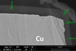
Modern barrier coatings such as PlasmaPlus® provide sensitive semiconductor components with reliable protection against moisture, migration, and a wide range of environmental influences. The atmospheric, ultra-thin protective layer—typically only 700 to 1,000 nanometers thick—forms an effective shield around internal components. This advanced coating technology offers reliable protection against water and ionic contamination, ensures electrical insulation and long-term performance, and maintains high resilience under thermal and mechanical stress. As a result, every IC package remains fully functional and electrically stable, even under the most demanding environmental conditions.
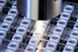
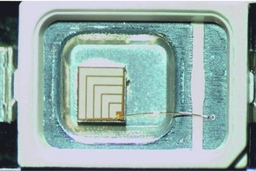
Final Assembly Cleaning & Marking
The advantages of this approach become immediately clear: end products remain completely free of particles and residues all the way to the delivery point, ensuring the highest standards of cleanliness and precision.
At the same time, secure and permanent marking can be applied to any surface, guaranteeing traceability and durability. By minimizing scrap, you achieve maximum yield, making processes both efficient and cost-effective.
Throughout production, process reliability and comprehensive quality assurance are maintained,right up to the final step. Only with clean, optimally prepared end products can true production reliability be ensured, allowing you to consistently deliver perfection and exceed customer expectations from start to finish.

